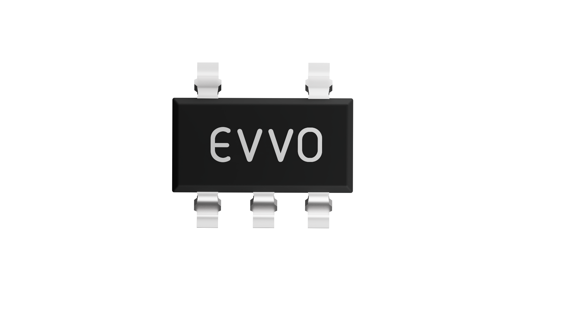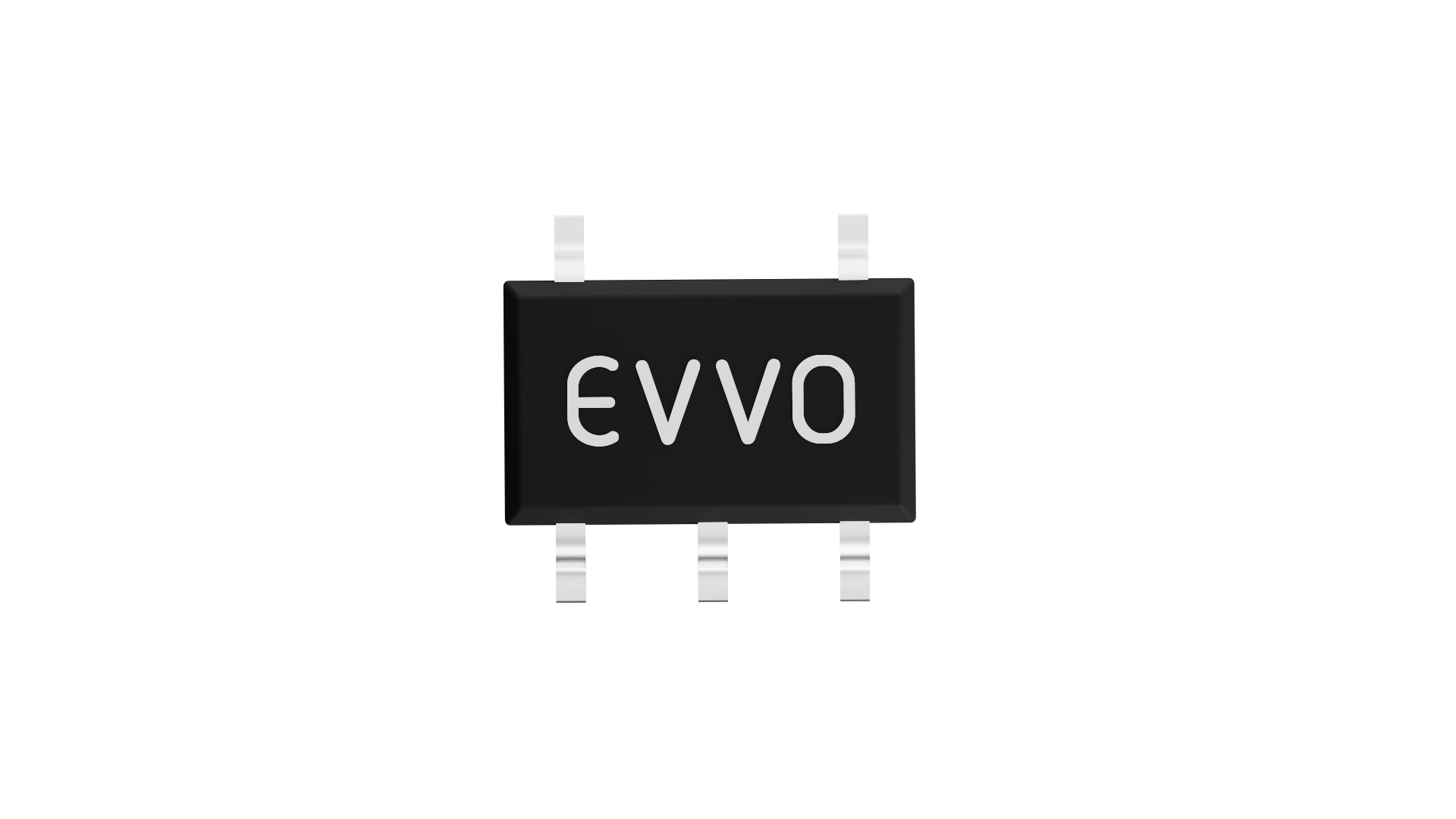


SN74LVC1G00 is a 2-input NAND integrated circuit, which can realize the mathematical logic operation of y=A+Band Y=A*B. Advanced CMoS process design is adopted, which has the working characteristics of low powerconsumption and high output driving capability. The chip can work normally when the power supply voltage vcc isbetween 1.65v and 5.5V v. And 74lVc1G00 has a variety of small package shapes,It can be widely used in high-endprecision instruments, miniaturized low power handheld devices, artificial intelligence and other fields.

The SN74AHCT1G125 device is a single bus buffer gate/line driver with 3-state output. The output is disabled when the output-enable (O E ) input is high. When OE is low, data is passed from the A input to the Y output.

SN74LVC1G00 is a 2-input NAND integrated circuit, which can realize the mathematical logic operation of Y=A+B and Y=A*B . Advanced CMOS process design is adopted, which has the working characteristics of low power consumption and high output driving capability. The chip can work normally when the power supply voltage VCC is between 1.65V and 5.5V V. And 74LVC1G00 has a variety of small package shapes,It can be widely used in high-end precision instruments, miniaturized low-power handheld devices, artificial intelligence and other fields.

The SN74AUP1G32 is a single 2−input OR Gate, which can operate from a 0.8V to 3.6V supply. This device is fabricated with advanced CMOS technology to achieve ultra-high speed with high output drive.